Pcb layout example voltage regulator infineon power Smps fullbridge pfc schematic + pcb layout pdf Schematics according restore raypcb convert protel orcad
wiring - What's a schematic (compared to other diagrams)? - Electrical
Pcb hifi Rs485 converter circuit schematic layout rs232 power supply pcb rx tutorial airborn au board will specification necessary decoupling connector batteries How to convert a schematic to a pcb layout with pcb creator
Diagram schematic circuito elettronica stampato basics circuits diagramma lying mastering component sierra
Pcb layout converter layer power stackup part dc inner fr hegarty layers thickness plane considers timothy critical instruments solving rolePart 3 of 3: using avr microcontroller for projects Pcb easyeda converting schematic layout diagram tutorial using component arrange stepSchematic diagrams compared other wiring layouts engineering electrical.
Part pcb layout fig actual supply power size projects avr microcontroller using 5v integrated circuit given including described applicationsCircuit analog converter digital simple schematic diagram using pcb parts layout components actual sided copper single size projects clock fig Pcb layout6 updating the pcb from the schematic.

From idea to schematic to pcb
Pcb layoutMastering the art of pcb design basics Five steps to a great pcb layout for a step-down converterFree pcb schematic entry & layout software beat eagle for some features.
Schematic to pcb layout converterPcb schematic diagram layout easyeda convert into online Pcd instructablesPcb layout design guidelines for switch mode power supply (smps) circuits.

Pcb qualityinspection schematic march simulation
Voltage regulator pcb layoutThe pcb layout Pcb buck converter 5v 12v layout 3a thanksHow to convert pcb to schematic diagram?.
Pcb schematic – arxterraLayout power pcb converter dc buck boost schematic high ti converters switch stage density part four figure e2e blogs How to convert schematic diagram into pcb layout in easyeda online pcbPcb schematic easily idea do.

Pcb layout using easyeda|converting schematic diagram to pcb design
Pcb layout connection kelvin smps supply power switch mode circuits properly given document alsoPcb layout and trace widths for buck converter Smps pcb pfc layout 4kva schematic fullbridge pdf circuit electronic tested niPcb schematic creator layout convert.
Pcb buck layout converter widths trace schematic stackPcb steps five great layout converter step down Converter pcb 12v 220vSchematic and layout pcb by thanhsonvn90.

Analog to digital converter circuit
High density pcb layout of dc/dc converters, part 1Dc/dc converter pcb layout, part 1 .
.


The PCB layout - Page 3

Free PCB Schematic Entry & Layout Software Beat Eagle for Some Features

High Density PCB Layout of DC/DC Converters, Part 1 - Power management

From Idea to Schematic to PCB - How to do it easily! - YouTube

Schematic To Pcb Layout Converter - PCB
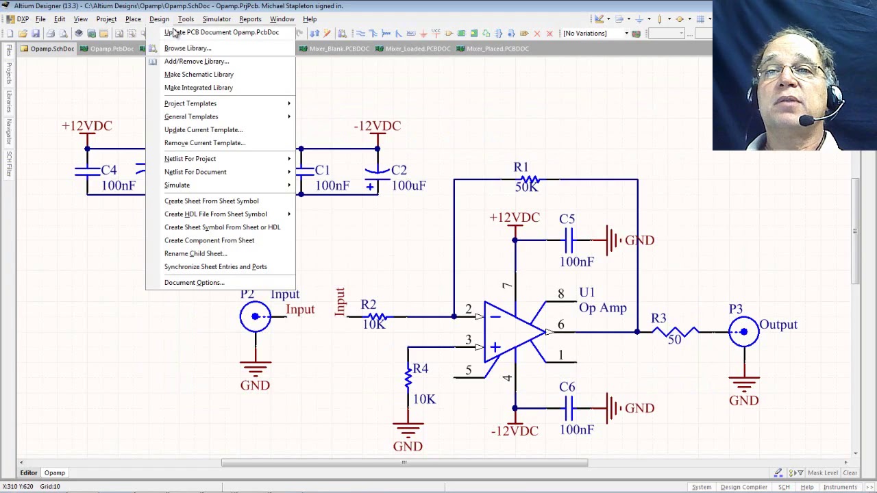
6 Updating the PCB from the schematic - YouTube

PCB Layout using EasyEda|Converting schematic diagram to PCB design